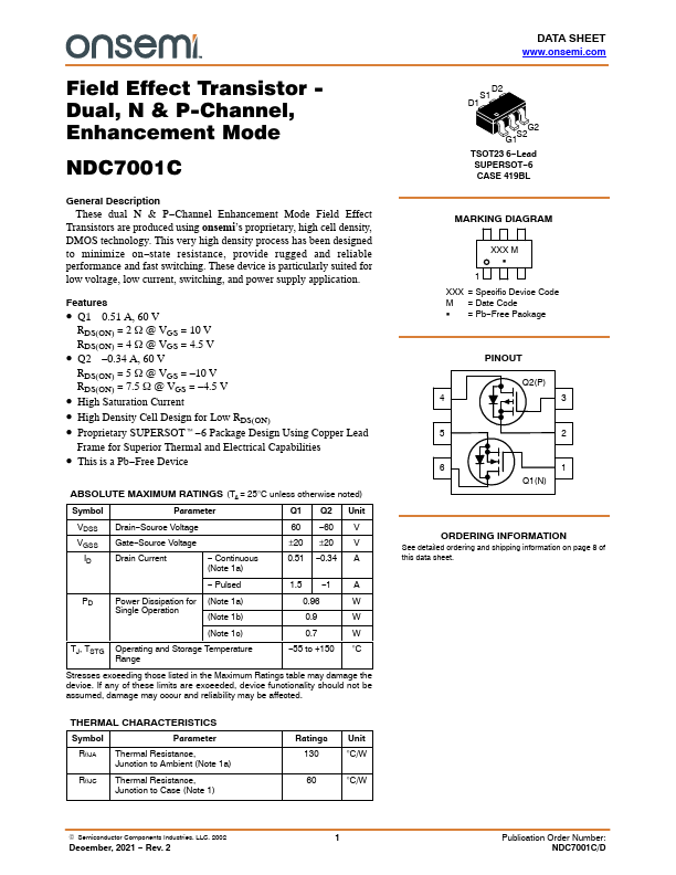
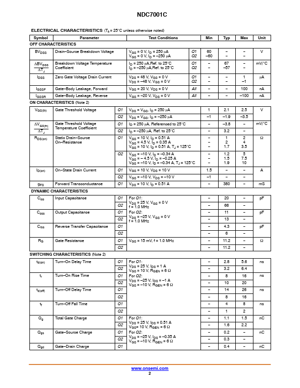
Datasheet4U Logo Datasheet4U.com

NDC7001C - Dual N&P-Channel MOSFET

Datasheet Summary

Description

These dual N & P

Transistors are produced using onsemi’s proprietary, high cell density, DMOS technology.

state resistance, provide rugged and reliable performance and fast switching

Features

  • Q1 0.51 A, 60 V RDS(ON) = 2 W @ VGS = 10 V RDS(ON) = 4 W @ VGS = 4.5 V.
  • Q2.
  • 0.34 A, 60 V RDS(ON) = 5 W @ VGS =.
  • 10 V RDS(ON) = 7.5 W @ VGS =.
  • 4.5 V.
  • High Saturation Current.
  • High Density Cell Design for Low RDS(ON).
  • Proprietary SUPERSOTt.
  • 6 Package Design Using Copper Lead Frame for Superior Thermal and Electrical Capabilities.
  • This is a Pb.
  • Free Device.

📥 Download Datasheet

Datasheet preview – NDC7001C

Datasheet Details

Part number NDC7001C
Manufacturer ON Semiconductor
File Size 359.51 KB
Description Dual N&P-Channel MOSFET
Datasheet download datasheet NDC7001C Datasheet
Additional preview pages of the NDC7001C datasheet.
Other Datasheets by ON Semiconductor

Full PDF Text Transcription

Click to expand full text
Field Effect Transistor Dual, N & P-Channel, Enhancement Mode NDC7001C General Description These dual N & P−Channel Enhancement Mode Field Effect Transistors are produced using onsemi’s proprietary, high cell density, DMOS technology. This very high density process has been designed to minimize on−state resistance, provide rugged and reliable performance and fast switching. These device is particularly suited for low voltage, low current, switching, and power supply application. Features • Q1 0.51 A, 60 V RDS(ON) = 2 W @ VGS = 10 V RDS(ON) = 4 W @ VGS = 4.5 V • Q2 –0.34 A, 60 V RDS(ON) = 5 W @ VGS = –10 V RDS(ON) = 7.5 W @ VGS = –4.
Published: |